
IBM 360
I have resumed work on the FPGA implementation of the IBM 360/65. I now have access to a complete set of IBM ALD's for the 7201-02 (the FAA 9020 customized version of the 2065 CPU), and because of that, I've decided to change how I'm implementing the CPU on the FPGA. Rather than working from the diagrams in the FEMDM (which are useful, but less detailed), I am now modeling the ALD's directly, which means that the emulation will be gate-level accurate.
The problem with modeling from the FEMDM, is that the diagrams in the FEMDM are representative of the circuits found in the CPU, but not accurate enough to base a simulation on. The ALD's show the actual AND, OR, and NOT gates, and are therefore much more accurate.
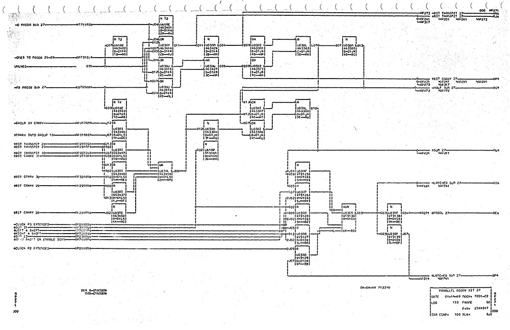
The XC5VLX110T FPGA has 17,280 logic slices available; 2,440 of these are taken by the PCIe interface (for I/O) and DDR2 controller (for main storage), and about 400 are taken by the shift registers to control the lamps and switches, leaving 14,440 for the CPU itself. Of the 3000+ pages of ALD's, I have identified 1315 that need to be translated into VHDL; I have completed 854 of these so far (although they still need lots of testing), and these take up around 5,200 slices. So, it's reasonable to expect that the finished CPU will occupy around 8,000-9,000 slices, which in turn means that the FPGA is very likely to be large enough for our needs.
- Details
This file pcie360_0_1_20120413.zip contains the VHDL code for the FPGA implementation of the 2065 emulator (incomplete, but capable of some elementary operations from the console panel). Here's the description from the top-level file (pcie360.vhd):
This is the design for an FPGA implementation of an IBM 2065 CPU emulator. As I have insufficient documentation on the IBM 2065, and because I don't have a copy of the ROS contents of the 2065, this is really an IBM 7201-2 CE emulator with 7201-specific bits stripped out.
Major subcomponents are:
- cpu - actual CPU emulation
- blinken - interface to an IBM 2065 console panel w/shift registers
- corememory - 256 KB of main memory (dual-ported between cpu and ioce)
- ioce - interface for the IOCE emulator running on the PC
- pcie - PCIE endblock to communicate with the PC (*)
This design is intended to be implemented on the Xilinx ML509 / XUPV5 developer board.
(*) A Xilinx PCI Express Endpoint Core example design needs to be added for this design to work. I cannot include that here because of copyright restrictions.
- Details
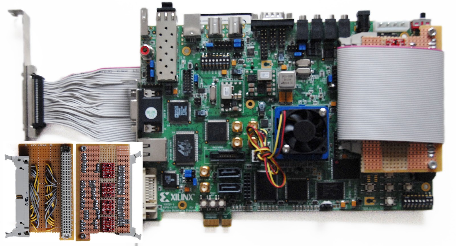
I realised that I'd need some extra hardware to connect the PCIe card to the console panel. The I/O pins on the Xilinx board operate at either 2.8 or 3.3 volts, and my console panel circuitry operates at 5 volts. So, what I need is some level shifters. I got four of these 4-way level shifters, and put them on a piece of veroboard with connectors for the Xilinx board and a 50-pin ribbon cable.
The 50-pin ribbon cable terminates in an HD50 connector (commonly used for narrow SCSI applications) on a PCI bracket. The panel has been fitted with the same connector, so a SCSI cable can be used as an interconnect between the PC and the panel.
- Details
Over the past few weeks, I've decided that there are a two things I don't like about the current 2065 emulator. These are:
- In the real 2065, several things would happen at once every 10 ns sub-cycle. The software emulator is necessarily much more sequential;
- The blinkenlights console doesn't get updated frequently enough.
Rather radically, I have therefore decided to change the emulator from a software emulator into a hardware emulator. Inspired by Lawrence Wilkinson's model 30 emulator on an FPGA, I'm going to implement the 2065 emulator on an FPGA as well.
The idea is to have the 2065 CPU and memory, as well as the logic to control the console panel on the FPGA board. For now, I'm not going to implement channel I/O on the FPGA, in stead, the FPGA will be interfaced with a PC running a software emulator of the channel and other I/O hardware.
The interface between the FPGA and the sioftware I/O will need to be able to support the following actions:
- The FPGA tells the software to execute an IPL, START I/O, TEST I/O, HALT I/O or TEST CHANNEL command;
- The software has read and write access to main memory implemented on the FPGA board;
- The software signals interrupt status to the FPGA board;
- The FPGA board signals interrupt completion to the FPGA board.
The interface needs to be reasonably fast and reliable. I found that FPGA development boards are available that fit into a PCIe slot. I've selected the Xilinx XUPV5 board pictured above for this project, as it has ample logic, a PCIe interface, and I/O pins that don't use exotic connectors.
Next thing to do is to build a small interface to connect the XUPV5 to the shift registers that drive the console panel.
- Details
- YouTube:
After Chris Bigos (www.ibm360.info) put large parts of the 7201-02 Field Engineering Diagrams Manual online, I had enough information to get a little further again.
I estimate that the cpu emulation is now about 70% complete. (out of 513 uops, 346 have been implemented completely and correctly, another 36 have been implemented and are probably correct, 32 are partially implemented, and 114 have not been implemented). Of course, the remaining 30% is the toughest part, though some of the uops probably will never get used because they're specific to the 9020's CE (7201-02) inter-processor communications and FAA special instructions.
I've had to use a few kludges, such as inserting uops into the microcode, keeping track of what the instruction counter should be, and faking the division and multiplication instructions, because some of those details are still vague. They should become less vague now that Chris has also put up the Field Engineering Theory of Operations Manual.
I've modified the "plain" Hercules emulator to write register values and a memory checksum to a text file after each instruction, and I'm doing the same in the M65 emulator. By comparing the text files, discrepancies between the emulators show up. The M65 emulator generates a second (huge) textfile that show the uops that get executed. I find the offending instruction in that second file, and try to figure out what causes the behavior to be wrong. This way, I'm now getting correct behavior IPL'ing OS/360 MFT up to the first message being written to the console. The console is an emulated 1052. The printer/keyboard has been replaced with a serial terminal in this emulation.
I would like to connect a 1052 to the emulator; that would make the interaction a lot more realistic. However, I think getting my hands on a real 1052, and somehow interfacing it to a PC is going to be difficult. I do have a german teleprinter (Telex), so I'm thinking of building a converter between RS232 and current-loop to hook that up to the pc running the emulator. I'll need to fix the teleprinter's power supply first though.
Well, enough said for now. Here's the video:
- Details
- YouTube:
I have some very exciting news to share. The emulator connected to the console panel has just run a rudimentary IBM 360 program.
Chris Bigos has provided me with ROS listings and control field definitions for the IBM 7201, an improved version of the model 65 used in the IBM 9020 complex, which was developed for the FAA for air traffic control.
Based on that information, I've put together a partial (very incomplete) emulator that is capable of running a simple 2-instruction program that counts up from 0. The program can be toggled in from the console panel.
The new emulator sources can be found on the wiki at http://ibm360-console.wikispaces.com/emulation.
Here's a short movie of the counting emulator
- Details
I've put a first version of the beginning of the emulation code on the Wiki at http://ibm360-console.wikispaces.com/emulation. Based on the information Chris has provided so far, I think I have a fair idea of what the emulation loop needs to look like. Only a few of the many micro-orders, and none of the actual ROS contents have been filled in.
- Details
I've updated the microachitecture Wiki with some information that Chris Bigos provided me with at his site. He provided me with scanned sections of some of the field engineering docs. I was able to add information to the microarchitecture, ROS and working registers entries. A big thank-you to Chris.
- Details
So here it is, the plans for the software that I promised on New Year's Eve.
Rather than writing an emulator from scratch (something I've done a few times before, see ES40 and FreeAXP for examples) I'm going to modify an existing emulator, the Hercules System/370, ESA/390, and z/Architecture Emulator. Whew, that's a mouthful! It emulates an IBM 370 or later rather than a System/360, but as the 370 was downwards compatible, OS/360 will run on Hercules.
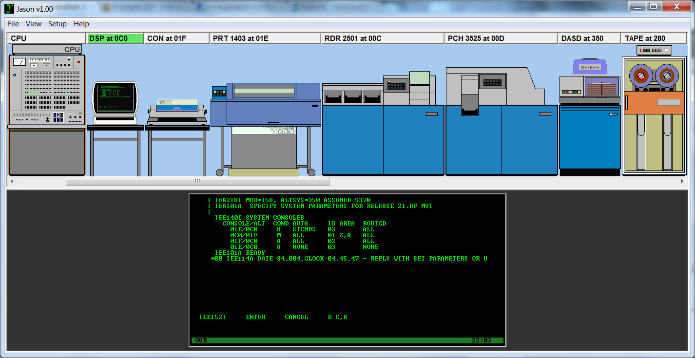
I like using Hercules with an add-on application called Jason. Jason is a graphical front-end to Hercules, that provides you with a view of the (virtual) devices attached to the emulator. It allows you to change a tape, or load a deck of cards using the mouse on the devices, rather than typing commands at the Hercules prompt. Having a Jason display running on an LCD panel next to the console panel seems to be a good way to show the rest of the 360 environment.
I'll make two modifications to Hercules. The most obvious change will be to equip Hercules with an interface to the real console panel. The more subtle change will be to replace the emulated 370 CPU with an emulated 360 model 65 CPU. The feasibility of doing this depends on my ability to find the proper documentation on the model 65's microarchitecture (see the Wiki for an overview of the microarchitecture).
The emulated cpu will no longer execute one entire System/360 instruction at a time, but one ROS microprogram instruction. Depending on the setting of the console panel switches, after pressing the START button, the system will keep executing instructions, execute a single System/360 instruction, or execute a single microprogram instruction.
- Details

First of all, hapy new year to all fellow tinkerers, collectors and enthousiasts!
I've set up a Wiki at http://ibm360-console.wikispaces.com/ with information about the model 65 microarchitecture. Hopefully, I can find the information to keep adding to it to build a complete picture of the model 65 microarchitecture. If you're familiar with 360's, or have suggestions as to what certain bits might mean, feel free to join the wiki and contribute.
- Details
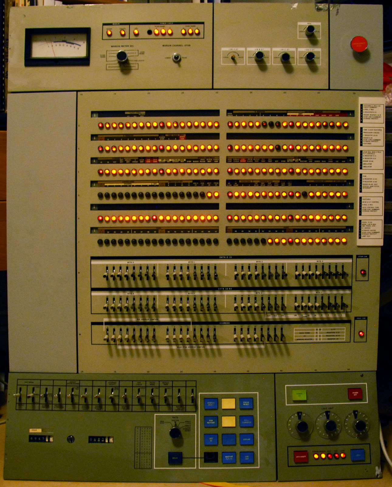
The hardware part of the project is more or less finished (one knob needs reattaching in a way that will make it stay on, and one lamp is missing). The picture on the left shows the mounting plate for the new electronics package, the right picture shows the electronics installed inside the panel (and running).
An impression of the end result is shown below. The VT100 may become the console terminal for the IBM (yes, it's as bad a mismatch as any, but I don't have any IBM terminals). The laptop below the panel is controlling it. All the lamps, switches and other controls now work flawlessly.
My apologies for the quality of the picture, it's dark here now, and a flash wouldn't bring out the beauty of the lit lamps.
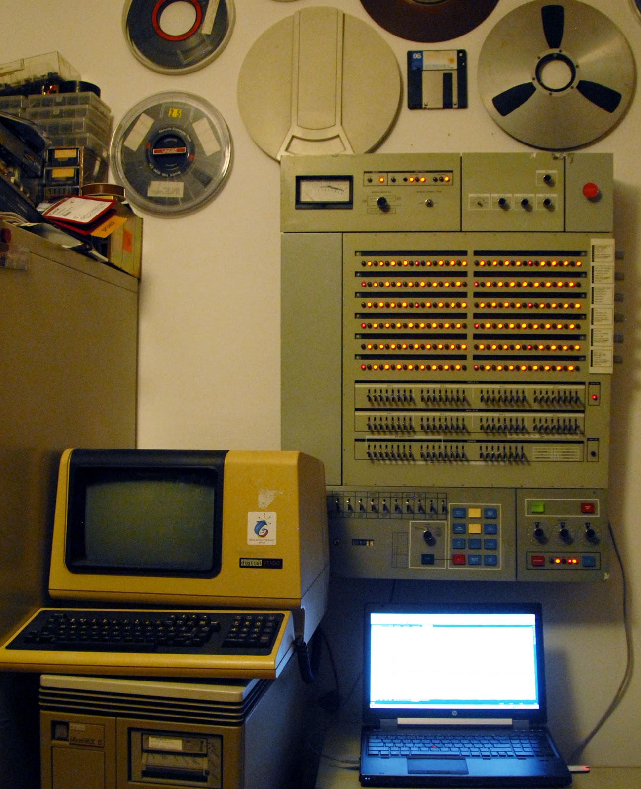
Of course, the panel isn't capable of anything useful until the software has been written. More on this in my next post.
- Details
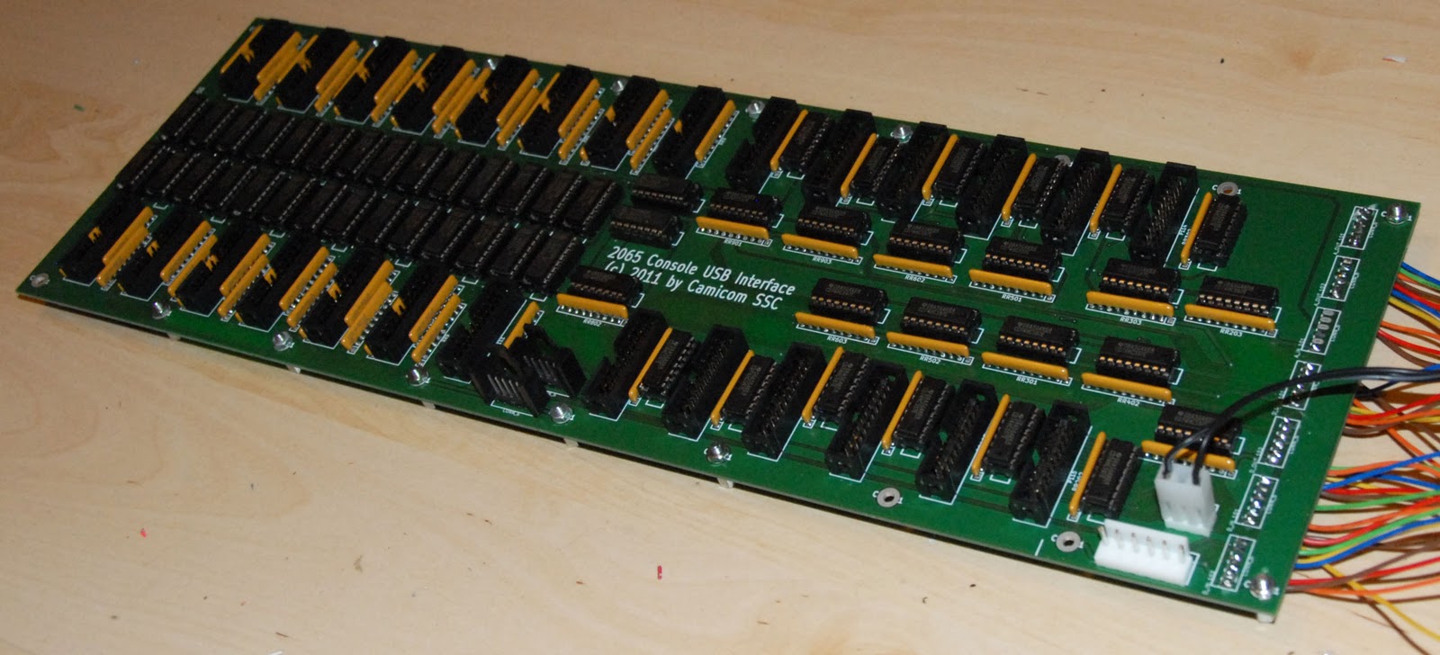
I've completed the board with the new electronics package. If you compare it to the prototype (shown below), the new board looks much neater, and will more easily fit inside the panel, leaving enough space for the cables.
The next job is to mount the new board inside the panel.
- Details
The PCB has shipped. It should arrive tomorrow or Friday, after which I'll have some work to do again.
In order to have a faithful emulation, I'll need to write an emulator that implements the microarchitecture of the Model 65. To this end, I'll need some documentation. I've posted the following in the IBM Historic Computing forum on LinkedIn:
A friend of mine who was a software engineer at Digital Equipment Corporation gave me a console panel for a System/360 model 65 that they had in their office (the console panel, not the system).
I am restoring the console panel, and I'm creating an interface to a PC to make all the lights and switches work as originally intended.
I'm now looking for field engineering documentation in order to make the emulation as faithful as possible to the original. These are some of the document titles I'm looking for:
- System/360 Model 65, 2065 Processing Unit, Field Engineering Maintenance Manual
- System/360 Model 65, 2065 Processing Unit, Field Engineering Diagrams Manual
- System/360 Model 65 Field Engineering Manual of Instruction
- System/360 Model 65 Field Engineering Theory of Operation Manual
- System/360 Model 65 CPU and Channels Training, Field Engineering Education Supplementary Course Material
The same material for the model 60, 62 or 67 in stead of the 65 would help too, given the similarities between these machines.
One thing in particular that I'm looking for that would help a lot is a data flow diagram showing the register and bus names. Another thing that would be very useful is a listing of the BCROS microcode.
The functional characteristics manual doesn't offer the level of detail I'd like.
- Details
I have received some more pictures of the PCB board being made:
After applying the solder mask
This is where the first problem with the PCB's shows: the oval pads for the power connectors and connectors to the USB interface look ok on top of the board (they're on the left side of the board in the pictures above), but on the bottom side of the board (where they will be soldered) there's too much solder mask, so there's only a very small rim to solder to. This means I'll have to scrape off some of the solder mask. Fortunately, there aren't many pads like this. I'm not sure where it went wrong, but it's too late to do anything about it.
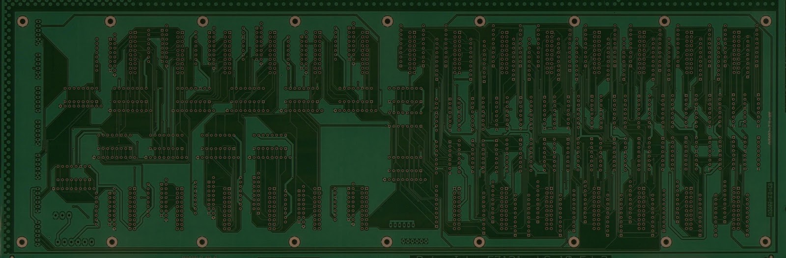
I just received a new set of pictures of the PCB manufacturing. The board is nearly finished now; the copper pads have been tinned, and the silkscreen printing has been applied:
- Details
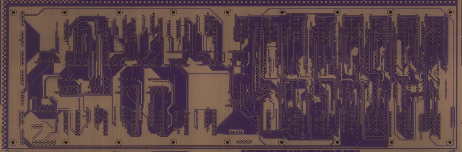
I just received photos of the PCB after the exposure step; all the holes have been drilled, and the PCB traces are visible:
- Details
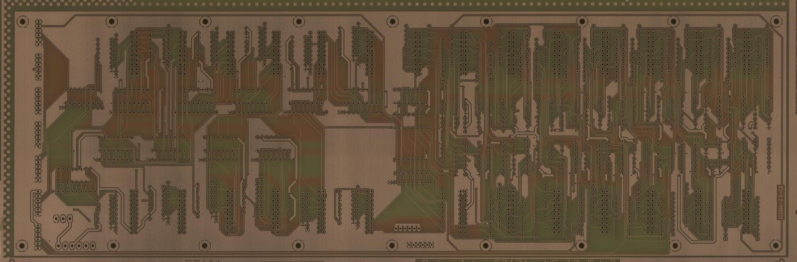
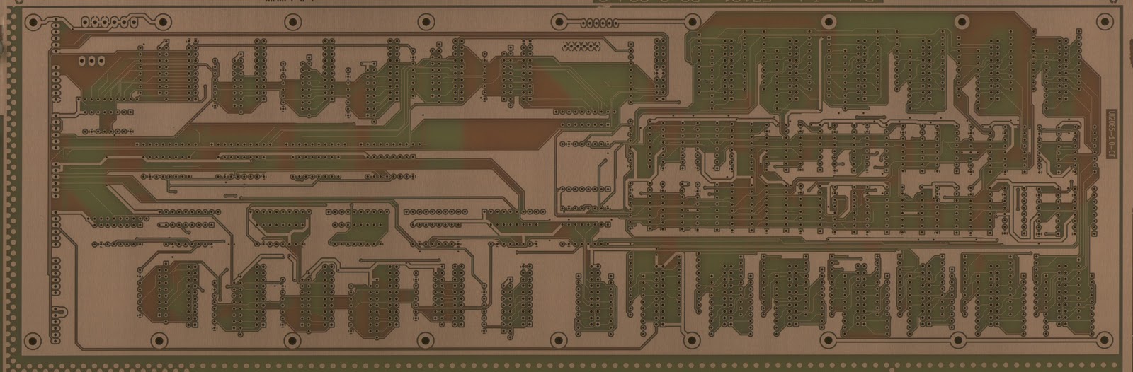
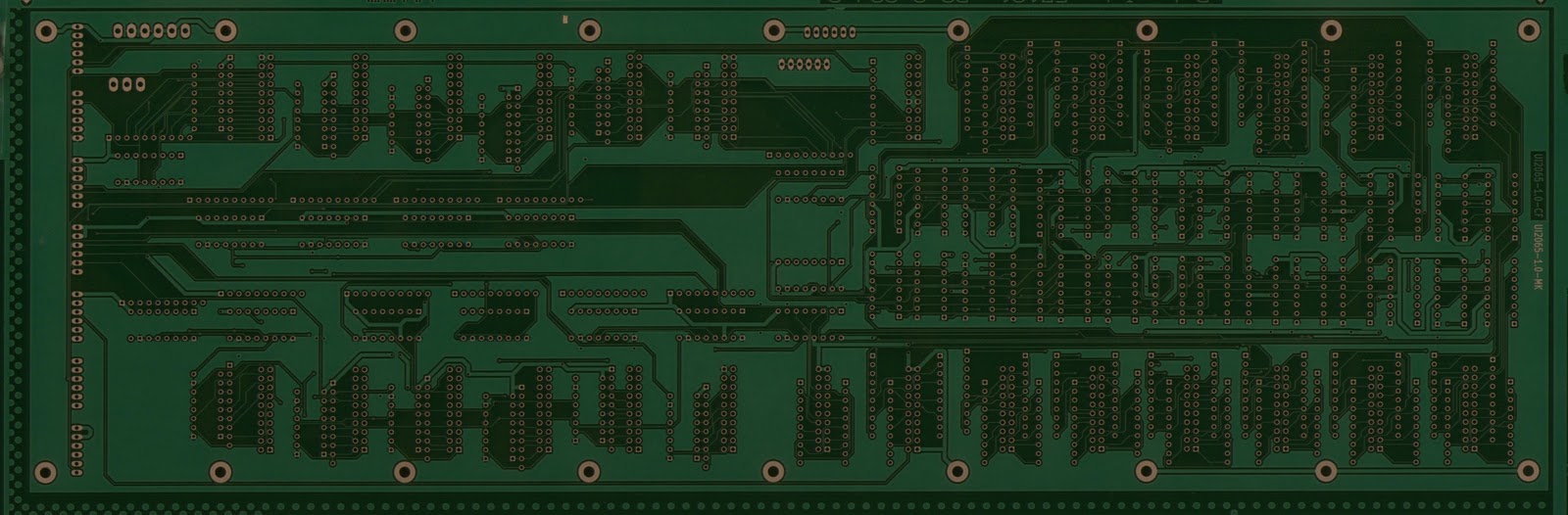
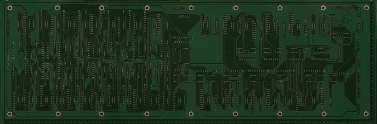
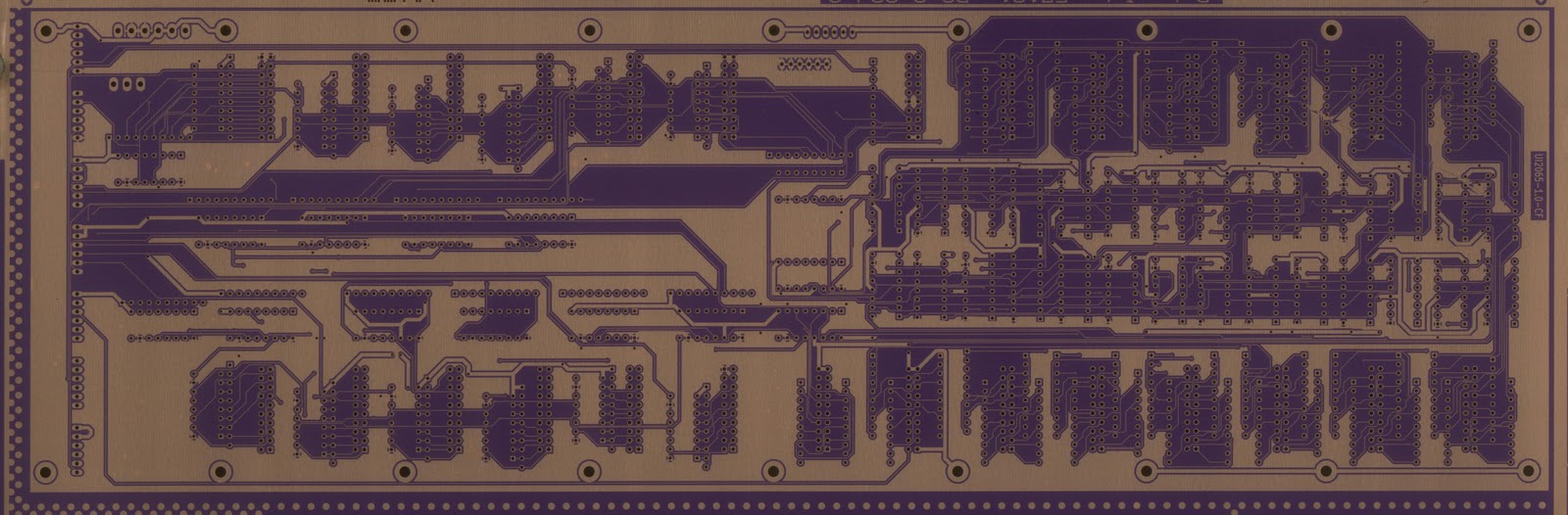
The PCB design has been finalized and sent off to a manufacturing company. It could take up to 8 working days to finish. A small setback was that the board as I originally designed it was too large for them, so I had to reduce the length to 43 cm. Of course they only tell you that the dimensions are too large when you try to actually place the order, not when you do the cost calculation on their website.
- Details
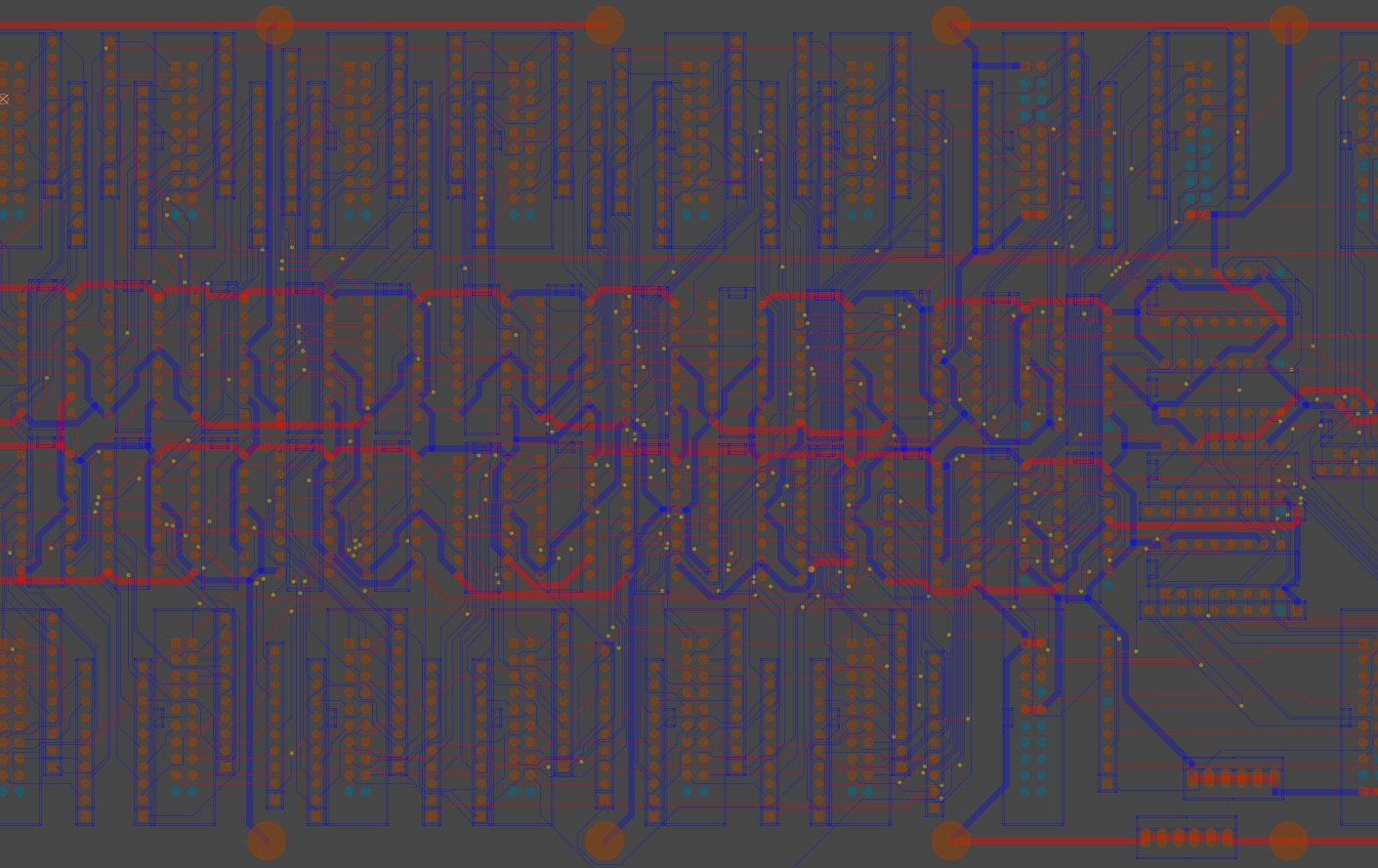
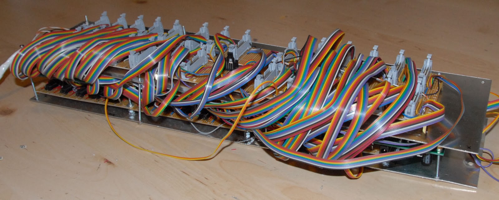
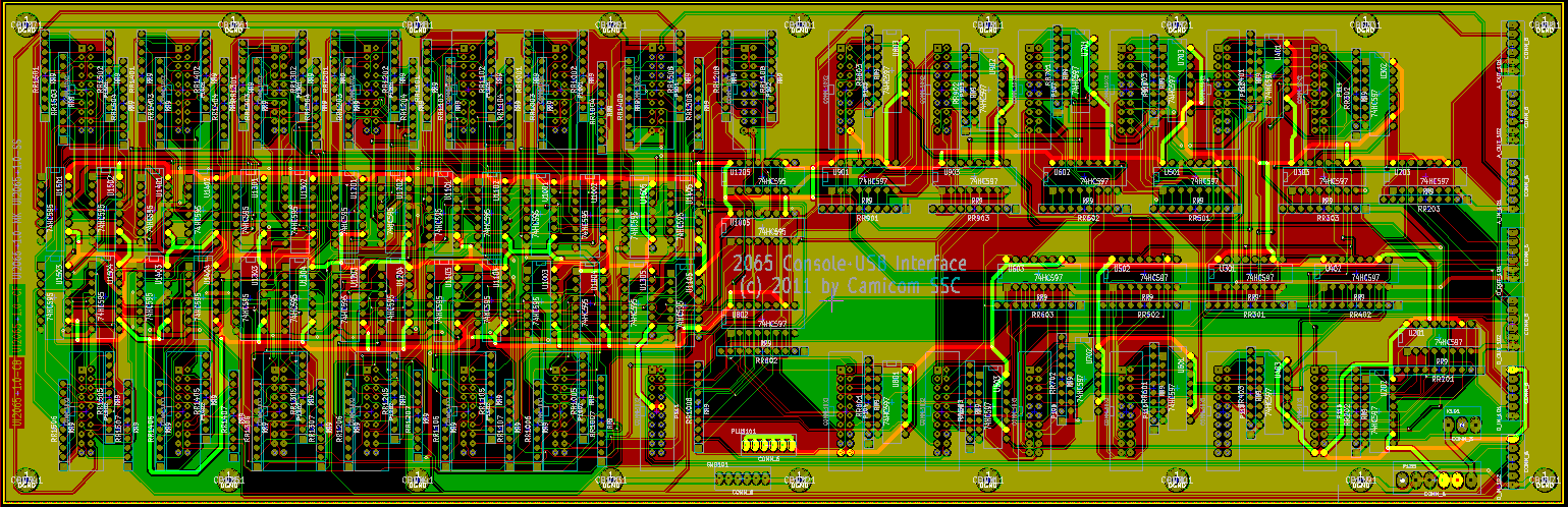
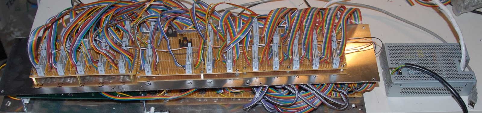
Debugging the veroboards with the pile of wires between them is proving challenging. I've therefore decided to let this be a prototype, and will re-implement the circuit on a printed circuit board. I've redrawn the schematics in kicad, including the actual connectors this time. The autorouter is now very busy getting it all to neatly fit a single 14 by 58 cm pcb. This will make for a much cleaner and thinner electronics package that will fit the panel without sticking out in the back.
- Details
Even though it's not entirely working yet, at least we have some decoration just in time for Christmas! Some of the lamps don't light while others light all the time. Time for more troubleshooting again...
Some of these problems come in groups: the first 16 lamps on output # 6 don't light up, the first 16 lamps on output # 7 light up all the time, and the first 24 lamps on output # 8 don't light up. These are the last 2, 2 and 3 chips on those outputs, so I'm sure I messed up output board number 2 in a somewhat consistent manner (it almost has to be the connection from one shift register to the next). 172 out of 235 lamps are working perfectly.
Not all switches are completely working either. Five pairs are ganged together (shorted somewhere), and one plainly doesn't work at all.
- Details
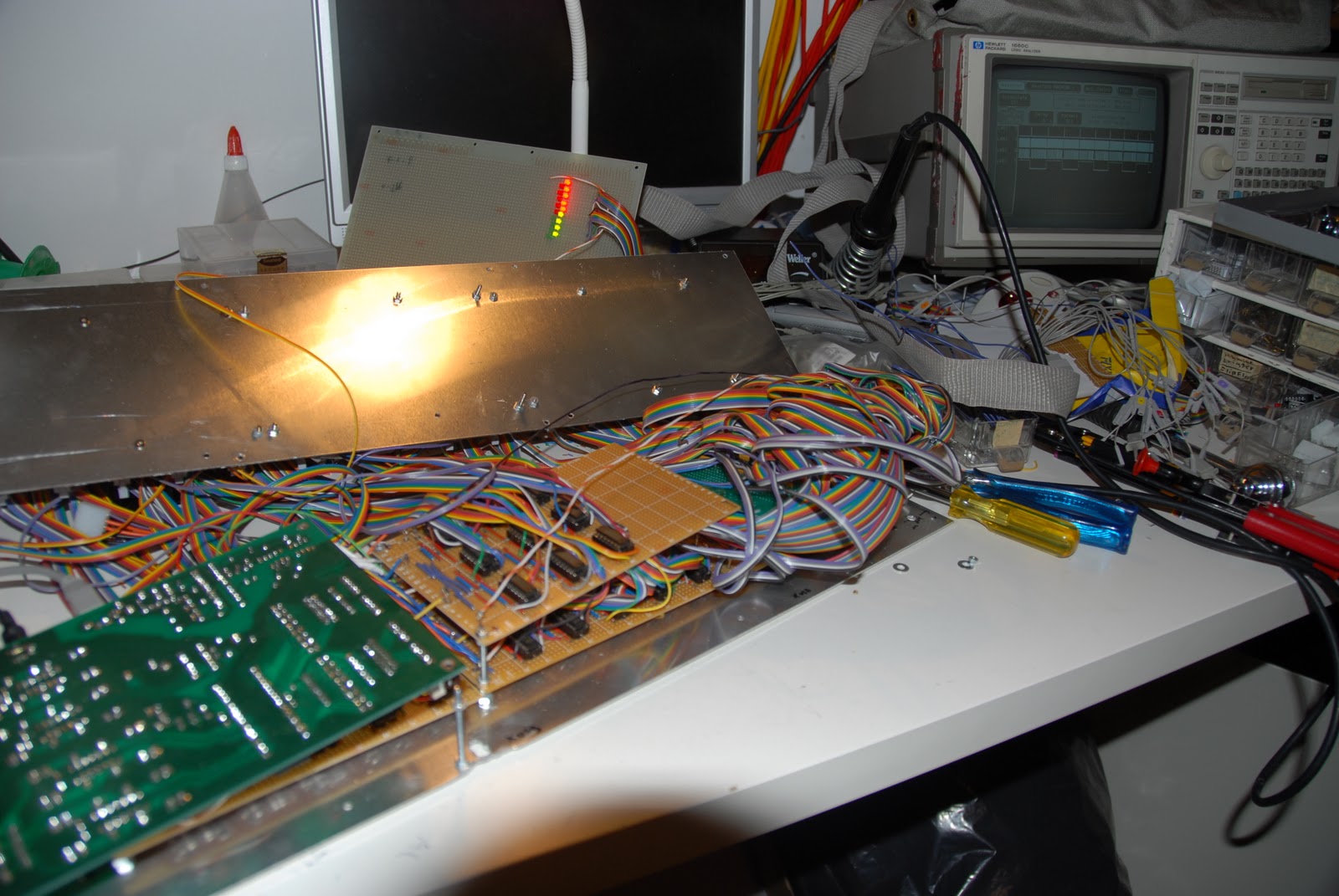
The electronics package is now complete. So, after an initial inspection for obvious problems (no shorts between +5v and ground for instance), it's time to try it out.
I put 18 LEDs on a board along with a flat cable with an IDC connector. I wrote a simple program that would flash all outputs on and off in a checkers pattern. I hooked it all up and... nothing...
So, that means time for troubleshooting. The first problem I found was a short between the CLOCK signal and the +5v on one of the input boards. A tiny amount of solder bridged two tracks on the veroboard. Then I found that the outputs on the Velleman kit needed pull-up resistors. I added those, found out that the outputs were inverting, changed the test program accordingly, and... still no success... Then I found out that I had crossed the outputs to the CLOCK and LATCH signals. I changed the test program to swap those two signals, and voila, the lights started flashing. Next up is testing and if necessary troubleshooting the inputs.
Btw, who else thinks logic analyzers are a godsend?
The electronics package now works correctly. The inputs didn't work yet, but I found out that the latch signal was active low. I changed the programming again, and that now works too. The outputs still work with the altered programming, because the output latches are edge triggered.
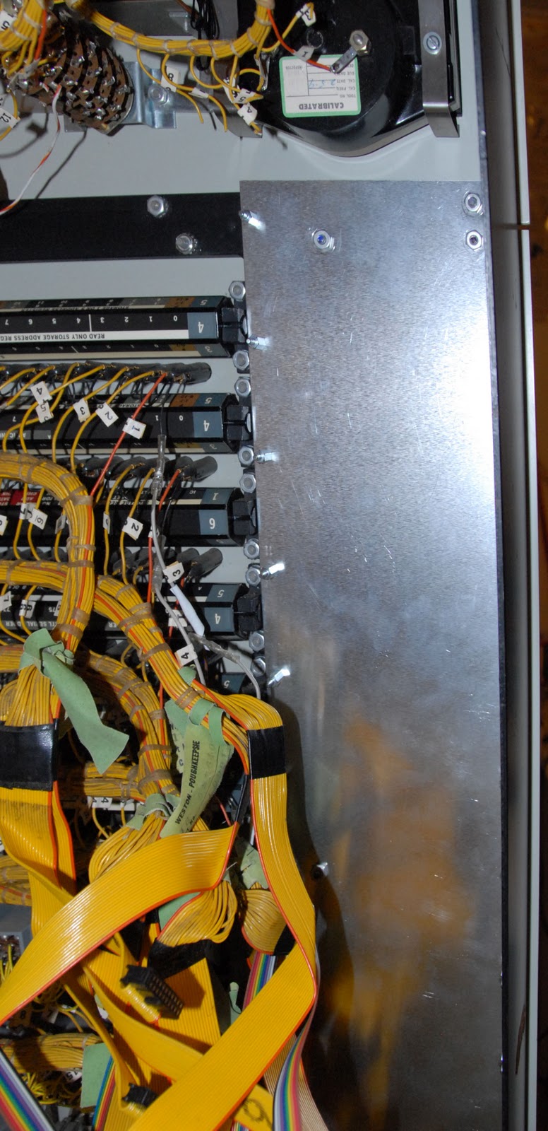
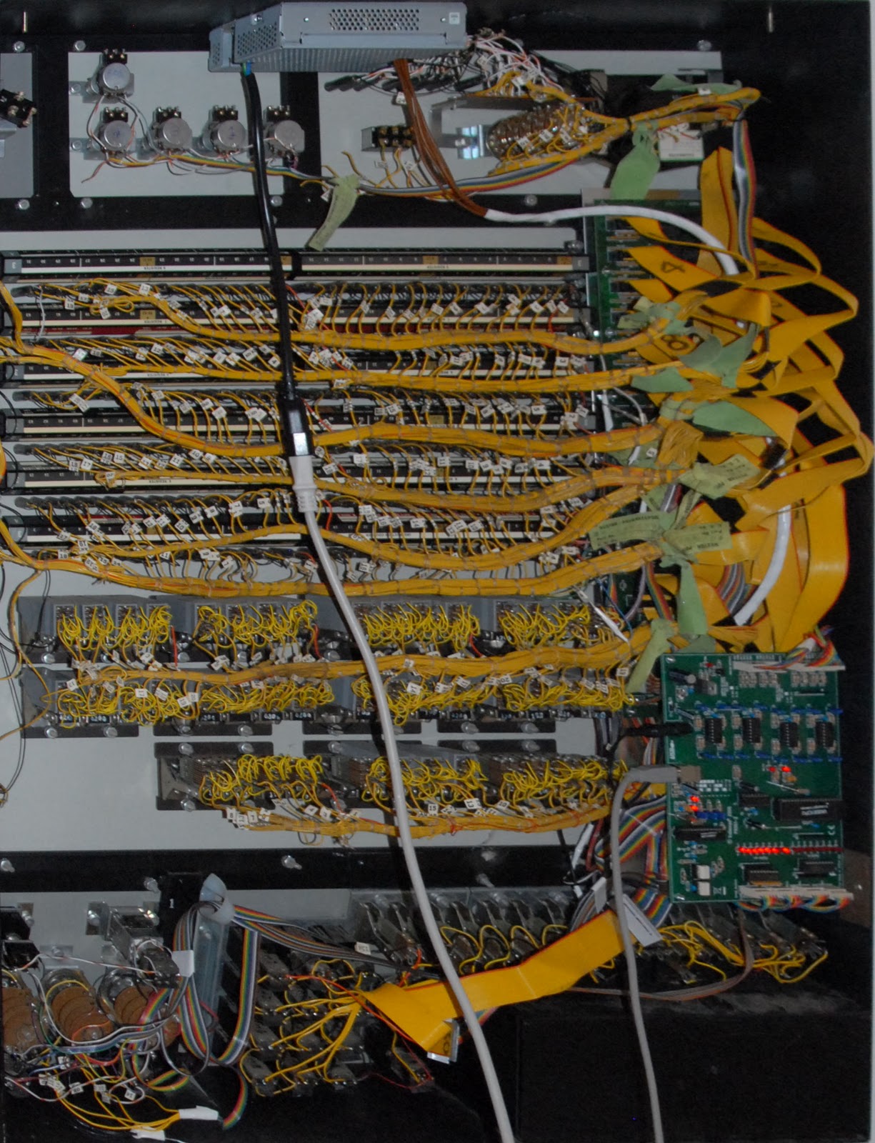
As you may or may not be able to see in the picture above, The electronics are mounted in two layers of pcb's on an aluminium panel that fits behind the blank panel of the IBM console. The pcb's with the connectors are mounted on a second aluminium panel. I now need to sandwich the two aluminium panels together. To this end, I need some long helical ridges wrapped around steel cylinders, which necessitates making a trip to the hardware store to get some (bolts, that is).
- Details