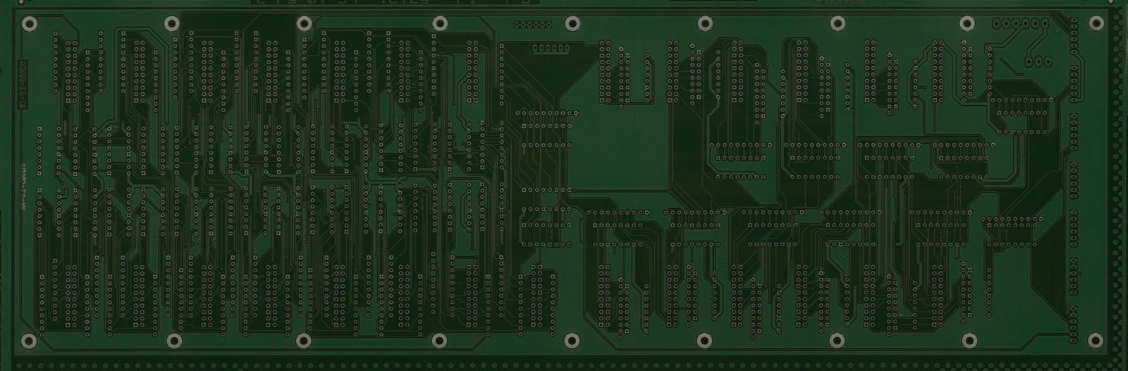
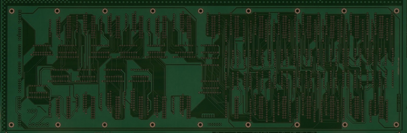
I have received some more pictures of the PCB board being made:
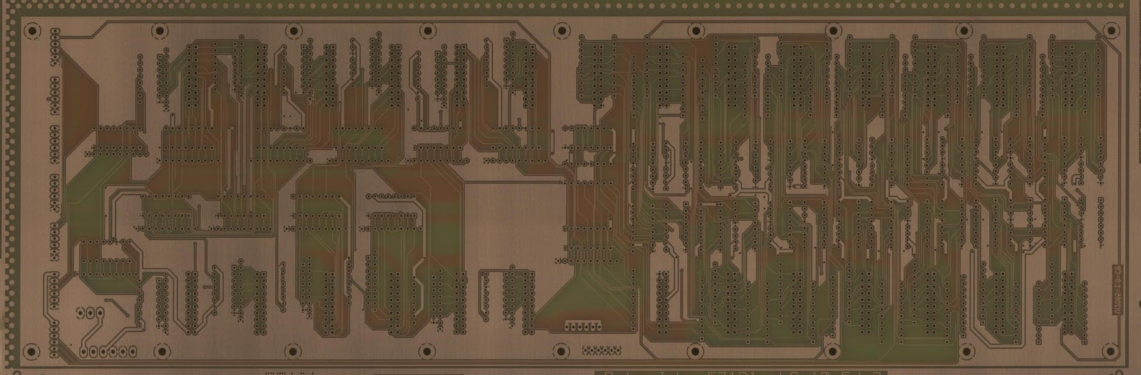
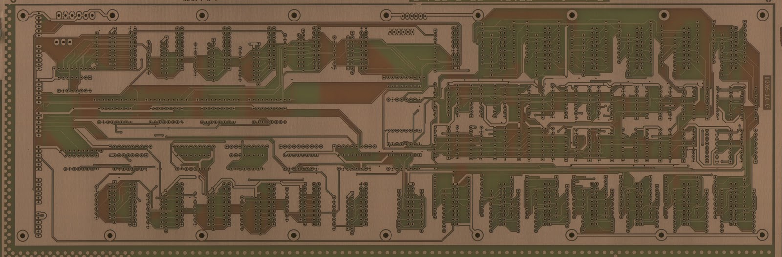
After applying the solder mask
This is where the first problem with the PCB's shows: the oval pads for the power connectors and connectors to the USB interface look ok on top of the board (they're on the left side of the board in the pictures above), but on the bottom side of the board (where they will be soldered) there's too much solder mask, so there's only a very small rim to solder to. This means I'll have to scrape off some of the solder mask. Fortunately, there aren't many pads like this. I'm not sure where it went wrong, but it's too late to do anything about it.
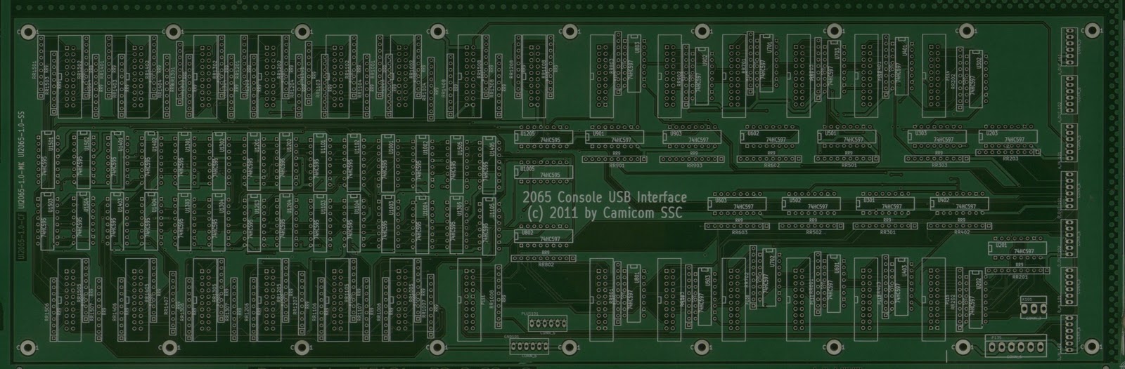
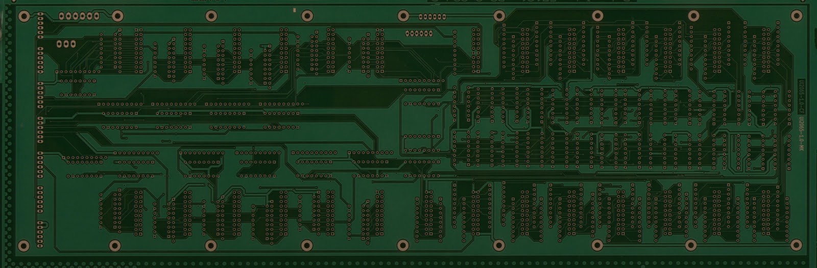
I just received a new set of pictures of the PCB manufacturing. The board is nearly finished now; the copper pads have been tinned, and the silkscreen printing has been applied: