*** UPDATED 24-APR-2017 ***
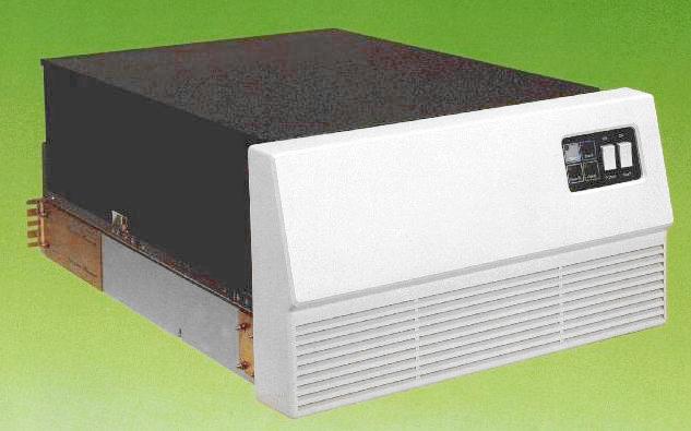
Almost a new year, time for a new project. Since the Convex C1 XP and Convex C1 XL I'm getting are missing their primary hard drive, I need to replace it with something. These systems are quite picky about what disks they support, but even if they weren't, working disks with an SMD (Storage Module Drive) interface are becoming somewhat rare. One disk I am sure these systems support is the Fujitsu M2351 ("Eagle") pictured above.
At the time (1980s) these disks were blazingly fast, with transfer rates around 2 MB per second, but today, they should be fairly easy to emulate using an FPGA.
I'm going to do something I haven't done before, and that is to include a microprocessor core into my FPGA design. Since I'm working with Xilinx FPGAs and tools, it's going to be a MicroBlaze processor.
A block diagram of the solution I'm thinking of is depicted below: 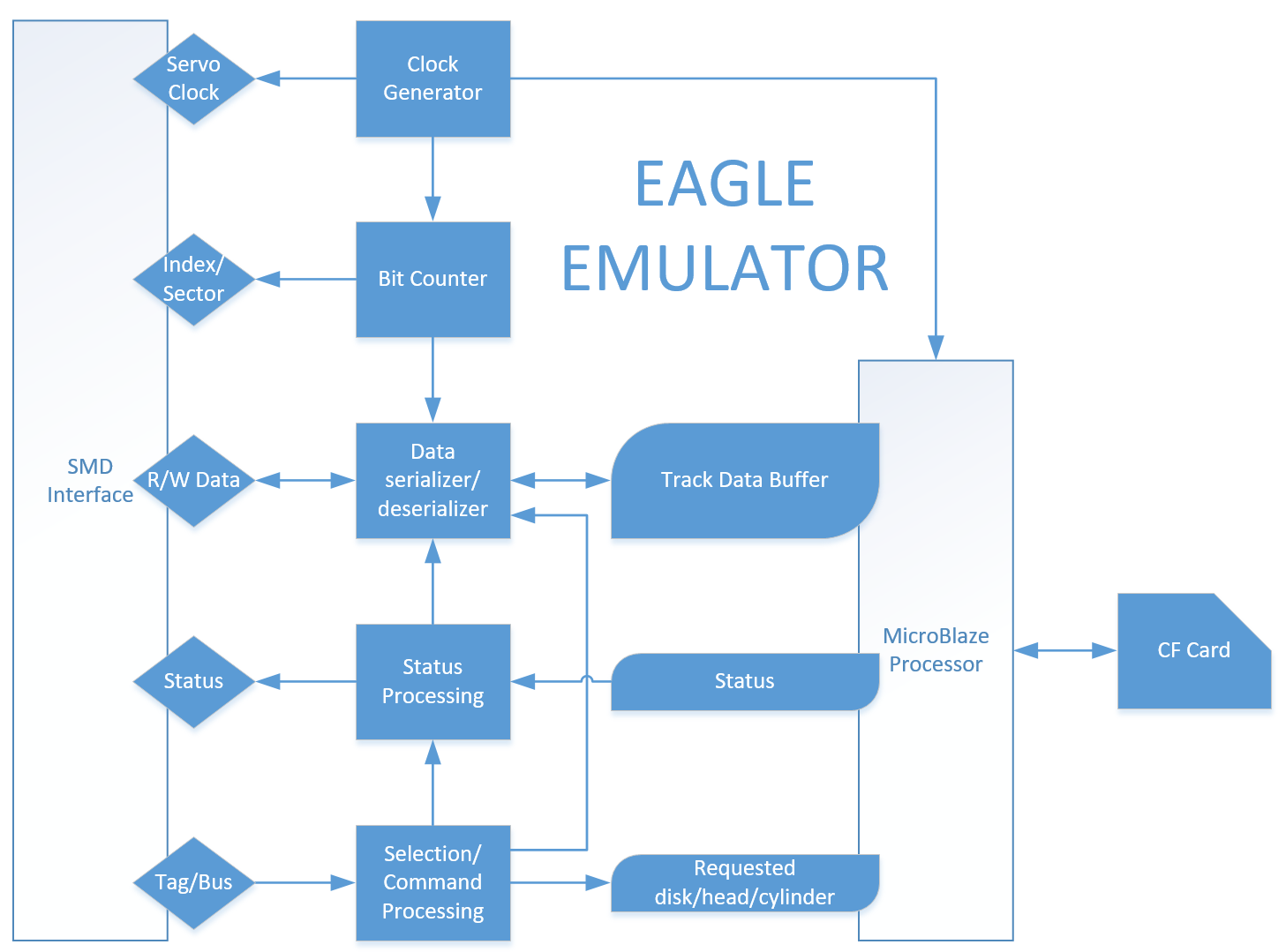
At the heart of the emulation is a dual-ported memory buffer large enough to hold an entire track worth of data, plus information about whether or not this data is "dirty" (has changed). The emulated disk writes and reads data to and from this buffer. A simple program running on the embedded MicroBlaze processor makes sure the buffer always contains the correct data for the currently selected track. To this end, the FPGA logic provides the processor with a register ("request register") where it can read what disk is currently selected (eventually, we should be able to emulate 4 or even 8 disks with a single FPGA), which head on that disk is selected, and which cylinder to seek to. The processor sends status data to the FPGA logic through a second register ("status register"), which indicates whether the buffer contains the data for the correct disk, head and cylinder or not.
Read/write operations are a continuous cycle of:
- The disk controller selects a disk, head, and cylinder using the bus and tag lines
- The selection and command processing engine in the FPGA interprets these commands and fills the "request register" with the requested disk/head/cylinder
- The MicroBlaze program sees that the requested disk/head/cylinder has changed, and proceeds to:
- Updates the "status register" to reflect that the buffer does not contain the requested data
- Scans the data buffer for any dirty data
- If it finds dirty data in the buffer, writes this data back to the CF card
- Fills the data buffer with the correct data from the CF card
- Updates the "status register" to reflect that the buffer now contains the requested data
- In the mean time, the status processing engine in the FPGA has indicated to the controller that the drive is not ready, and is blocking the clock signals to the controller
- As soon as the "status register" shows that the correct data is in the buffer, the status processing engine indicates to the controller that the drive is ready and on-cylinder, and allows the flow of clock signals to the controller
- The bit counter in the FPGA simulates the rotation of the disk, providing addressing data to the bit serializer/deserializer, and providing index and sector pulses to the controller
- The disk controller uses the tag and bus lines to initiate a read or write action
- The selection and command processing engine in the FPGA interprets these commands, and activates the bit serializer (read) or deserializer (write) engine.
- The bit serializer reads data from the buffer and sends it to the controller
- The bit deserializer receives write data from the controller, and writes it to the buffer, marking the buffer as dirty in the process.
The only electronics external to the FPGA card are going to be some level shifters, and bus interfaces to get from the FPGA's 2.5v single-ended logic to +/-5v differential logic as used on the SMD interface.
Update, 24-APR-2017
The SMD emulator is coming along nicely. It's no longer strictly an Eagle emulator, as I found out that my Convex was configured with NEC 2352 disk drives (500 MB), so I'm emulating one of those now instead. I did have to make a few changes to my initial design though, mainly because interfacing with the CF-card through the ACE controller is just way too slow. One of the first things I did was change the design to use an SD card instead, and get rid of the MicroBlaze processor. Instead, I used a simple 4-wire SD-card controller in VHDL, using the SPI protocol.
Unfortunately, that is also too slow, and the disk controller does not like it if it takes a lot of time (~150 ms) to select another head. So, I changed things to use a larger track buffer, one that can hold the data for all the surfaces in one cylinder at the same time. Unfortunately, this no longer fits the Block RAM resources in the FPGA, so I had to use the external SRAM on my Xilinx development board. That worked fine, but now the track-to-track seek time was about 6 seconds, which - again - causes timeouts on the disk controller end.
So, the final idea is to use a buffer that can hold the contents of the entire disk. The Xilinx development board I'm using (XUPV5) has a DDR2 SODIMM socket, so I populated that with a 2GB SODIMM. The final design looks like this:
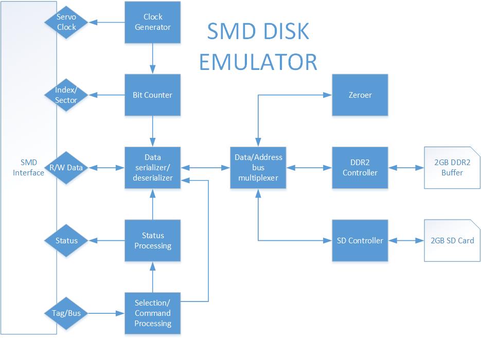
The idea is that when you start the disk emulator, the RAM first gets filled with 0's (the "Zeroer" block in the diagram). You can then either put the (empty) disk online, or push a button to load the contents from the SD card (a further idea would be to add a selection switch so you can have multiple images on a single SD card), then put the disk online. After the computer is done with the emulated disk, you put the disk off-line, then press a second button to write the image to the SD card. Loading the image from the SD card takes about 40 minutes, writing it back takes about 60 minutes. I may spend some time looking for a usable full 4-bit SD-protocol controller that will bring these times down, but I'm not really worrying about that now.
The prototype hardware looks like this:
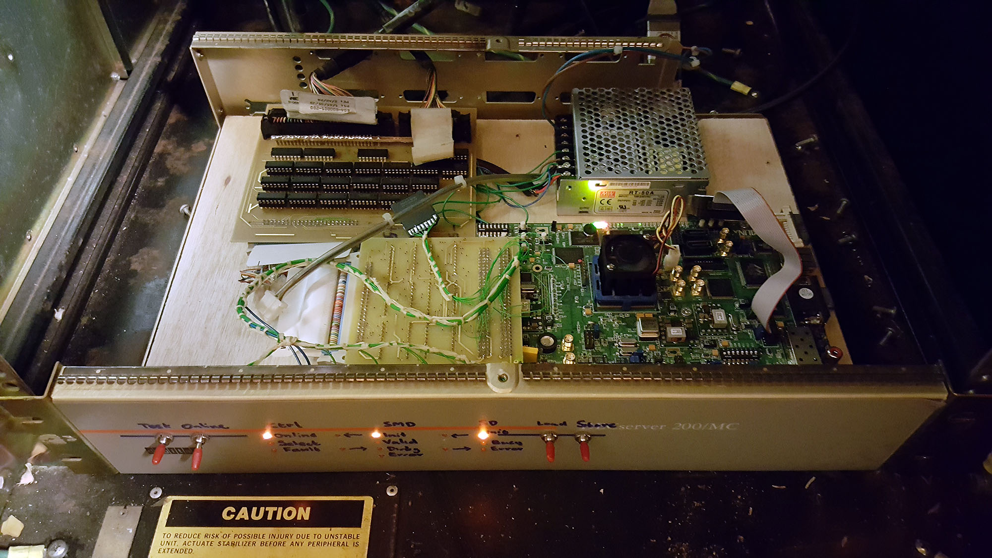
It's housed in the chassis of a broken DECserver 200. On the front panel, from left to right are:
- A switch to enable the tester (not shown in the block diagram, this is an excerciser that continuously writes test patterns to RAM and reads them back, lighting the "FAULT" LED when there's a mismatch. I added this, because I found that it was very easy to get the DDR2 controller to misbehave (very timing sensitive).
- A switch to put the drive online. If the Zeroer or SD Controller is still active, the disk will come online after that operation is done.
- Three LEDs representing the controller interface status; "ONLINE" indicates the disk is online, "SELECT" indicates the controller has selected the disk, and "FAULT" indicates that the disk is signalling an error to the controller.
- Two LEDs showing read/write activity between the disk and controller
- Four LEDs representing the state of the DDR2 buffer memory; "INIT" indicates memory has been initialized (Zeroer has finished), "VALID" indicates that a disk image has been loaded from the SD card, "DIRTY" indicates data has been written to the buffer that has not been saved to the SD card yet, and "ERROR" indicates that data could not be read or written in time.
- Two LEDs showing read/write activity to the SD card
- Three LEDs representing the state of the SD card controller; "INIT" indicates the controller has recognized the SD card and is ready, "BUSY" indicates the SD card is currently being read or written, and "ERROR" indicates the controller detected a problem comunicating with the SD card.
- A switch to initiate loading a disk image from the SD card
- A switch to initiate storing a disk image to the SD card
Inside, all components are mounted on a bit of plywood. From the top right hand corner, clockwise:
- Power supply (+ 5V for the electronics, -5V for the balanced SMD interface lines, +12V for the fans)
- Xilinx XUPV5 FPGA development board (the ribbon cable is for the JTAG programmer interface)
- Universal level-shifter board, to translate between the FPGA's 3.3V interface and 5V TTL logic. Universal because I designed it some time ago, and I use the same board for multiple projects. The SD card holder (really a microSD-to-SD adapter with wires soldered to it) and the front panel are connected directly to the 3.3V pins on this board. The wires have been tied together in a neat 1960s style.
- SMD interface board with the balanced line drivers and receivers
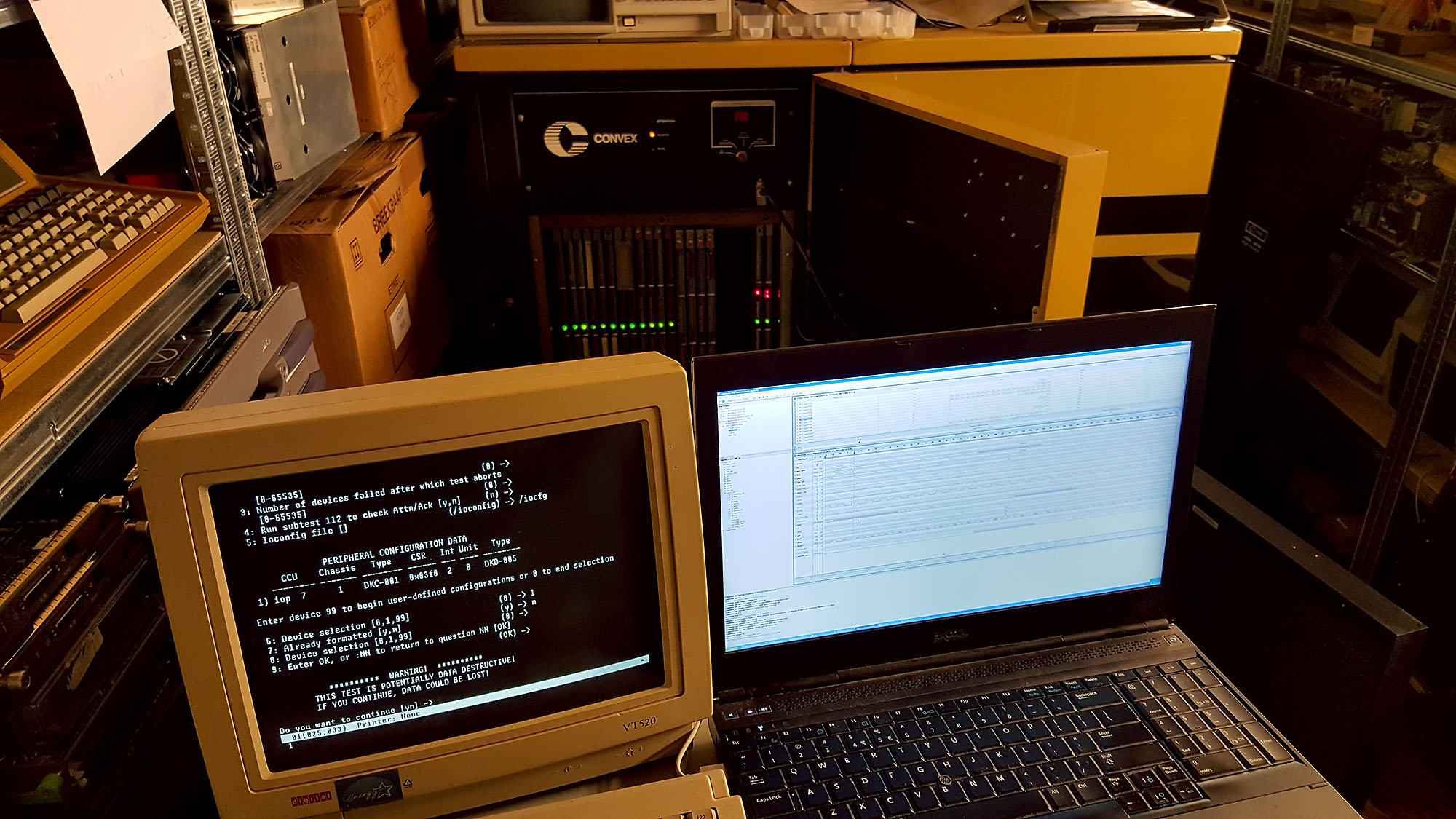
I'm still debugging the emulator, for this, I'm using the Convex, and the SPU diagnostic program for the Xylogics controller and SMD disks. There seems to be a problem where data is sometimes written to the wrong place in the track buffer, and I'm trying to sort this out. A typical debugging session involves using Xilinx' ChipScope software to look at various signals inside the FPGA, and sometimes it involves a real logic analyzer to look at the real signals. For this end, I have soldered a few wires with a 20-pin header connector to one of the Xylogics controllers. A typical debugging session might look like this:
